Using XILINX IP Core Block RAM (2)
2015-08-04 20:25
387 查看
Initial RAM
1) In order to download the *.bits file in to Xilinx FPGA,the way to initial RAM is using .coe file. We can load the .coe file to initial RAM when we configured the IP Core.The .coe file syntax is shown below .
MEMORY_INITIALIZATION_RADIX=16;
MEMORY_INITIALIZATION_VECTOR=
00 19 31 4a 61 78 8e a2
b5 c5 d4 e1 ec f4 fb fe …
The value’s radix can be set in the *.coe file , the symbol and string will not allowed in this file.
2) In order to use Modelsim to simulate the program ,we need to use system function to read data from text file,such as .dat and .txt. In simulation ,we use the readmemhorreadmemb to read data into Memory type. Or using the *.mif file to initial RAM.
The ideal of search the correspond number
1) The way to find the correspond value is easier to find similar data,we can read data from RAM,and stored the result of (find_num - data) into a temporary Memory,after that check the result whether there is zero ,when the result is zero,output the address,it means data in this address is the number we want to find ,also we can use the counter to record the correspond number appeared how many times.if there is no correspond number then cnt return 0,else find the similar number in RAM.First,check the minimum number in temporary Memory.second,check the data in Memory if there is a number equal to the minimum number and counter it times.
2) There is differences in write data in to RAM between actual program and simulation.The way of initial RAM using *.coe file is not supported in modelsim,so we must write data into Memory through port A,the port B is only can be read in simple dual port RAM.Because of this difference we can not use simulation program to run in FPGA.
The framework of simulation and real program
1) Botth of two framework are use the same clk in port A and port B,so clka and clkb were both connected in mclk.the framework as shown in Figure 6 and Figure 7.
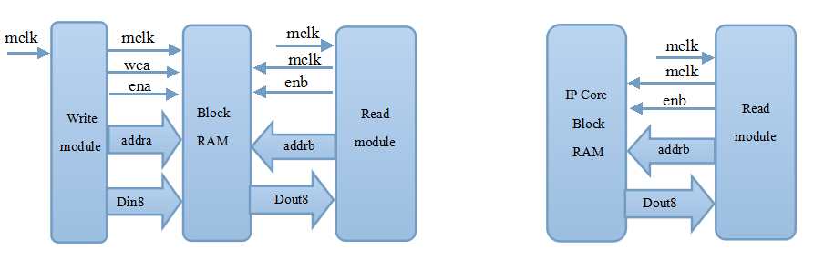
2) In simulation,the first step is read data from text through write module.and next ,write data into Block RAM ,finally read data from Block RAM in temporary Memory. In real program there is no need write process so the port A is unconnected.
Program For ISE Version
1) In order to download the *.bits file in to Xilinx FPGA,the way to initial RAM is using .coe file. We can load the .coe file to initial RAM when we configured the IP Core.The .coe file syntax is shown below .
MEMORY_INITIALIZATION_RADIX=16;
MEMORY_INITIALIZATION_VECTOR=
00 19 31 4a 61 78 8e a2
b5 c5 d4 e1 ec f4 fb fe …
The value’s radix can be set in the *.coe file , the symbol and string will not allowed in this file.
2) In order to use Modelsim to simulate the program ,we need to use system function to read data from text file,such as .dat and .txt. In simulation ,we use the readmemhorreadmemb to read data into Memory type. Or using the *.mif file to initial RAM.
The ideal of search the correspond number
1) The way to find the correspond value is easier to find similar data,we can read data from RAM,and stored the result of (find_num - data) into a temporary Memory,after that check the result whether there is zero ,when the result is zero,output the address,it means data in this address is the number we want to find ,also we can use the counter to record the correspond number appeared how many times.if there is no correspond number then cnt return 0,else find the similar number in RAM.First,check the minimum number in temporary Memory.second,check the data in Memory if there is a number equal to the minimum number and counter it times.
2) There is differences in write data in to RAM between actual program and simulation.The way of initial RAM using *.coe file is not supported in modelsim,so we must write data into Memory through port A,the port B is only can be read in simple dual port RAM.Because of this difference we can not use simulation program to run in FPGA.
The framework of simulation and real program
1) Botth of two framework are use the same clk in port A and port B,so clka and clkb were both connected in mclk.the framework as shown in Figure 6 and Figure 7.
2) In simulation,the first step is read data from text through write module.and next ,write data into Block RAM ,finally read data from Block RAM in temporary Memory. In real program there is no need write process so the port A is unconnected.
Program For ISE Version
module wr_rd_ram(
input  r_clk,     //clk 24Mhz
input  r_rst,
input  [7:0] r_dout,
output reg [11:0] r_addr,
output reg r_en,

output  [7:0] right_data_out,
output  [7:0] right_addr_out,
output  [7:0] right_cnt,

output  [7:0] similar_cnt,
output  [7:0] similar_data_out,
output  [7:0] similar_addr_out
);

parameter checknum = 8'h78;

reg [2:0] next;
reg rd_rdy,srh_dne;
reg [7:0] rd_mema [0:255];
reg [7:0] rig_cnt,sim_cnt;
reg [8:0] i,j,k,similar;
reg [7:0] rig_addr_tmp,rig_data_tmp,sim_addr_tmp,sim_data_tmp;

//Combinatial logic
always@(posedge r_clk) begin
if(r_rst==1'b0) begin
{next,r_addr} <= {3'd0,12'b0};
{r_en,rd_rdy} <= {1'd0,1'b0};
end
else
case(next)
3'd0: begin r_en <= 1'b1; next <= 3'd1; end
3'd1: begin
if(r_addr > 12'b1111_1111) begin
next <= 3'd3;
rd_rdy <= 1'b1;
end
else
next <= 3'd2;
end
3'd2: begin                //put result of (r_dout-checknum) in rd_mema
rd_mema[r_addr] <= (r_dout>checknum) ? r_dout-checknum:checknum-r_dout;
r_addr <= r_addr + 12'b1;
next <= 3'd1;
end
default: ;
endcase
end
//search  the correspond number in rd_mema
always@(posedge r_clk) begin
if(!r_rst) begin
{rig_cnt,i} <= {8'b0,9'd0};
{rig_addr_tmp,rig_data_tmp} <= {8'b0,8'b0};
end
else
if(rd_rdy) begin
if(i <= 8'd255) begin
case(rd_mema[i])
8'd0: begin
rig_data_tmp <= rd_mema[i];
rig_addr_tmp <= i;
rig_cnt <= rig_cnt + 1'd1;
end
default:;
endcase
i <= i + 8'd1;
end
end
end
// search  min  (checknum-r_dout)   in rd_mema
always@(posedge r_clk) begin
if(!r_rst) begin
{similar,j,srh_dne} <= {9'd257,9'd0,1'b0};
end
else
if(rd_rdy) begin
if(j <= 8'd255) begin
similar <= (similar < rd_mema[j])? similar:rd_mema[j];
j <= j + 8'd1;
end
else
srh_dne <= 1'b1;
end
end
//  find similar number
always@(posedge r_clk) begin
if(!r_rst) begin
{sim_cnt,k} <= {8'd0,9'b0};
{sim_addr_tmp,sim_data_tmp} <= {8'b0,8'b0};
end
else
if(srh_dne) begin
if(k <= 8'd255 ) begin
case(rd_mema[k])
similar:begin
sim_data_tmp <= rd_mema[k];
sim_addr_tmp <= k;
sim_cnt <= sim_cnt + 1'd1;
end
default:;
endcase
k <= k + 8'd1;
end
end
end
// output data and it's address
assign right_data_out = rig_data_tmp;
assign right_addr_out = rig_addr_tmp;
assign right_cnt = rig_cnt;

assign similar_data_out = sim_data_tmp;
assign similar_addr_out = sim_addr_tmp;
assign similar_cnt = sim_cnt;

endmodule

相关文章推荐
- PowerShell ISE中代码转换大小写的技巧
- Verilog文件格式范例
- ISE使用过程中遇到的一个诡异问题
- Verilog HDL语言不全面但基本入门够用介绍
- Verilog $Scannf 使用小结
- 关于FPGA逻辑设计的21个小贴士
- 关于FPGA逻辑设计的21个小贴士
- 关于Error: Can't compile duplicate declarations of entity "**" into library "work"的错误
- ISE中将Verilog封装为IPcore
- (筆記) 如何設計邊緣檢測電路? (SOC) (Verilog)
- 使用xilinx ip core FIFO First- World First-Through (FWFT)模式的注意事项
- 在EDK里面添加ISE IP core的方法
- Verilog 有符号数无符号数混用
- Partitioning for Synthesis
- 在Archlinux下安装Xilinx ISE12.3以及Digilent Adept的使用
- Veriog_Notes_Chapter 1
- Veriog_Notes_Chapter 2
- 升级思科WLC firmware详细步骤
- Cisco ISE + Windows Server 2008 实验