《CS:APP》 chapter 6 The Memory Hierarchy笔记
2014-07-16 15:24
267 查看
The Memory Hierarchy
6.1 Storage Technologies
The earliest IBM PCs didn’t even have a hard disk. 让我惊奇的是早期的IBM直接没有硬盘。。。6.1.1 Random-Access Memory
Random-access memory(RAM) comes in two varieties— static anddynamic . Static RAM (SRAM) is faster and significantly more expensive than Dynamic RAM(DRAM). SRAM is used for cache memories, both on and off the CPU chip. DRAM is used for the main memory plus the frame buffer of a graphics system.
Static RAM
SRAM stores each bit in a bistable memory cell. Each cell is implemented with a six-transistor circuit. This circuit has the property that it can stay indefinitely in either of two different voltage configurations, or states.
Dynamic RAM
DRAM stores each bit as charge on a capacitor. DRAM storage can be made very dense—each cell consists of a capacitor and a single access transistor. Unlike SRAM, however, a DRAM memory cell is very sensitive to any disturbance. When the capacitor
voltage is disturbed, it will never recover.
The trade-off is that SRAM cells use more transistors than DRAM cells, and thus have lower densities, are more
expensive, and consume more power.
Conventional DRAMs
The cells (bits) in a DRAM chip are partitioned into d supercells, each consisting of w DRAM cells. A d × w DRAM stores a total ofdw bits of information. The supercells are organized as a rectangular array with r rows
and c columns, where rc = d . Each supercell has an address of the form (i, j), where i denotes the row, and j denotes the column.
地址线和数据线分离,宽度是2bit的地址线的行列地址共用同一地址线分先后寻址。宽度是8bit的数据线在寻址确定后每次并行传输1byte的数据。
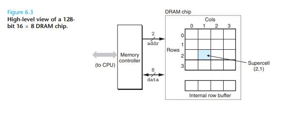
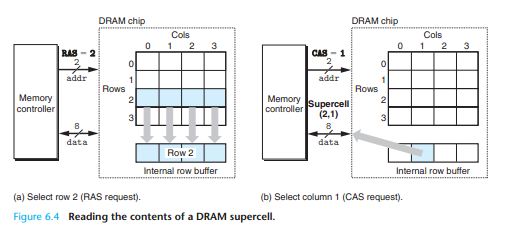
Notice that the RAS and CAS requests share the same DRAM address pins.
One reason circuit designers organize DRAMs as two-dimensional arrays instead of linear arrays is to reduce the number of address pins on the chip. The disadvantage of the two-dimensional array organization is that
addresses must be sent in two distinct steps, which increases the access time.
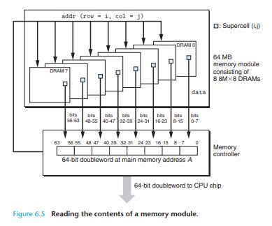
Memory module
Nonvolatile Memory
DRAMs and SRAMs are volatilein the sense that they lose their information if the supply voltage is turned off.
A programmable ROM(PROM) can be programmed exactly once. PROMs include a sort of fuse with each memory cell that can be blown once by zapping it with a high current.
An erasable programmable ROM (EPROM) .
An electrically erasable PROM(EEPROM) is akin to an EPROM, but does not require a physically separate programming device, and thus can
be reprogrammed in-place on printed circuit cards.
Flash memoryis a type of nonvolatile memory, based on EEPROMs, that
has become an important storage technology.
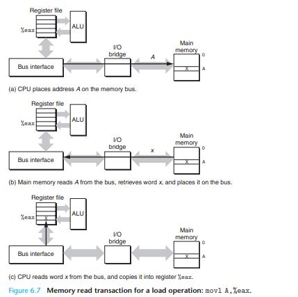
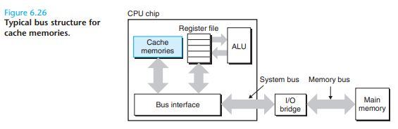
Accessing Main Memory
Each transfer of data between the CPU and memory is accomplished with a series of steps called abus transaction
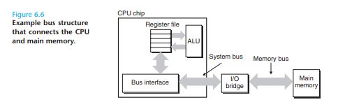
Different vendors develop different bus architectures as a way to differentiate their products. 比方说AMD和intel的板子I/O bridge的设计就不同。
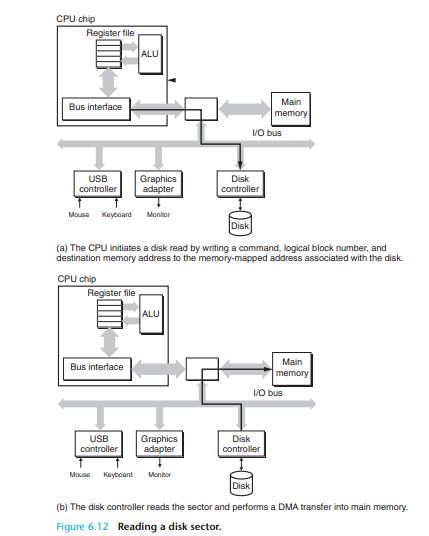
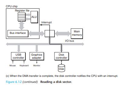
Consider what happens when the CPU performs a load operation such as
movl A,%eaxwhere the contents of addressA are loaded into register %eax.
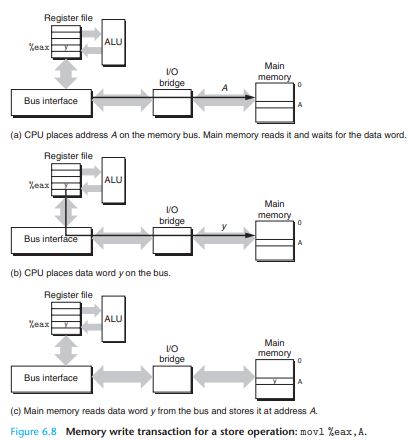
Conversely, when the CPU performs a store instruction such as
movl %eax,Awhere the contents of register%eaxare written to address A, the CPU initiates a write transaction.
6.1.2 Disk Storage
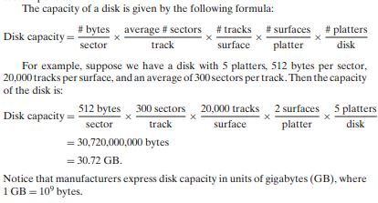
Disk Geometry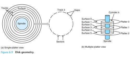
Disk operation
This mechanical motion is known as a seek . At any point in time, all heads are positioned on the same cylinder.
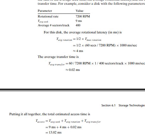
Seek time: To read the contents of some target sector, the arm first positions the head over the track that contains the target sector. The time required to move the arm is called the seek time.
The seek time, Tseek, depends on the previous position of the head and the speed that the arm moves across the surface. The average seek time in modern drives, Tavg seek, measured by taking the mean of several
thousand seeks to random sectors, is typically on the order of 3 to 9 ms. The maximum time for a single seek, Tmax seek, can be as high as 20 ms.
Rotational latency: Once the head is in position over the track, the drive waits for the first bit of the target sector to pass under the head. The performance of this step depends on both the position of the surface when
the head arrives at the target sector and the rotational speed of the disk.
The average rotational latency,Tavg rotation, is simply half of Tmax rotation
Transfer time:When the first bit of the target sector is under the head, the drive can begin to read or write the contents of the sector.
Connecting I/O Devices
Unlike the system bus and memory buses, which are CPU-specific, I/O buses such as PCI are designed to be
independent of the underlying CPU.
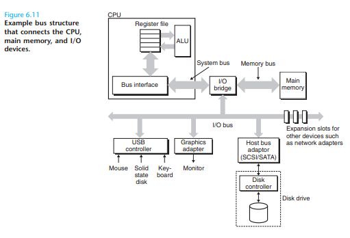
A Universal Serial Bus (USB) controller is a conduit for devices attached to a USB bus, which is a wildly popular standard for connecting a variety of peripheral I/O devices, including
keyboards, mice, modems, digital cameras, game controllers, printers, external disk drives, and solid state disks. USB 2.0 buses have a maximum bandwidth of 60 MB/s. USB 3.0 buses have a maximum bandwidth of 600 MB/s.
A graphics card (or adapter) contains hardware and software logic that is responsible for painting the pixels on the display monitor on behalf of the CPU. A host bus adapter that
connects one or more disks to the I/O bus using a communication protocol defined by a particular host bus interface .The two most popular such interfaces for disks are SCSI (pronounced “scuzzy”) and SATA (pronounced “sat-uh”). SCSI disks are typically faster
and more
expensive than SATA drives.
6.1.3 Solid State Disks
A solid state disk (SSD) is a storage technology, based on flash memory (Sec-tion 6.1.1), that in some situations is an attractive alternative to the conventional rotating disk.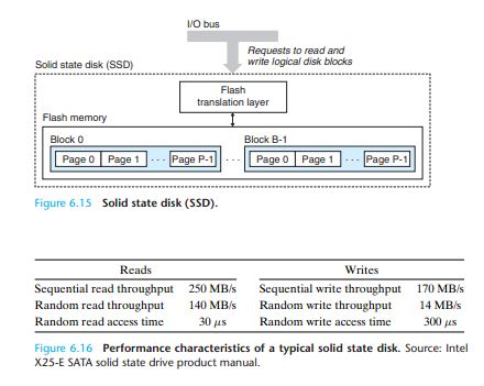
The difference between random reading and writing performance is caused by a fundamental property of the underlying flash memory. Data is read and written in units of pages. A page can be written only after the entire
block to which it belongs has been erased (typically this means that all bits in the block are set to 1).
Random writes are slow for two reasons.
First, erasing a block takes a relatively long time, on the order of 1 ms, which is more than an order of magnitude longer than it takes to access a page.
Second, if a write operation attempts to modify a pagep that contains existing data (i.e., not all ones), then any pages in the same block with useful data must be copied to a new (erased) block before the write to page
p can occur.
SSDs have a number of advantages over rotating disks. They are built of semiconductor memory, with no moving parts, and thus have much faster random access times than rotating disks, use less power, and are more rugged.
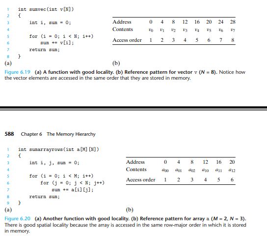
6.2 Locality
Programmers should understand the principle of locality because, in general, programs with good locality run faster than programs with poor localityAt the hardware level, the principle of locality allows computer designers to speed up main memory accesses by introducing small fast memories known as cache memories that hold blocks of
the most recently referenced instructions and data items
Similarly, the operating system uses main memory to cache the most recently used disk blocks in the disk file system.
好的locality和坏的locality的对比
关于数据和代码在CPU操作上的区别:
An important property of code that distinguishes it from program data is that it is rarely modified at run time. While a program is executing, the CPU reads its instructions from memory. The CPU rarely overwrites
or modifies these instructions.
Nonetheless, knowing how to glance at a source code and getting a high-level feel for the locality in the program is a useful and important skill for a programmer to master.
6.3 The Memory Hierarchy
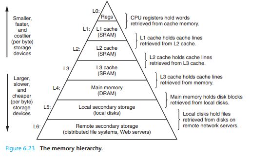
6.3.1 Caching in the Memory Hierarchy
Level K 就相当于 Level K+1的cache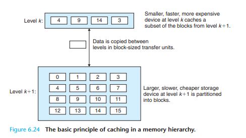
Cache Hits
When a program needs a particular data object d from level k + 1, it first looks for d in one of the blocks currently stored at level k .If d happens to be cached at levelk , then we have what is called a cache hit .
Cache Misses
If, on the other hand, the data object d is not cached at level k , then we have what is called a cache miss . When there is a miss, the cache at level k fetches the block containing d from the cache at level k + 1, possibly overwriting an existing
block if the level k cache is already full
6.4 Cache Memories
6.4.1 Generic Cache Memory Organization
Consider a computer system where each memory address has m bits that form M = 2^m unique addresses. As illustrated in Figure 6.27(a), a cache for such a machine is organized as an array of S = 2^s cache sets.Each set consists of E cache lines . Each line consists of a data block of B = 2^b bytes, a valid bit that indicates whether or not the line contains meaningful information, and t = m − (b + s) tag bits (a subset of the bits
from the current block’s memory address) that uniquely identify the block stored in the cache line.
In general, a cache’s organization can be characterized by the tuple (S,E,B,m). The size (or capacity) of a cache, C , is stated in terms of the ag-gregate size of all the blocks. The tag bits and valid bit are
not included. Thus, C = S × E × B .
Cache lines, sets, and blocks: What’s the difference?
It is easy to confuse the distinction between cache lines, sets, and blocks. Let’s review these ideas and
make sure they are clear:
A block is a fixed-sized packet of information that moves back and forth between a cache and main memory (or a lower-level cache).
A line is a container in a cache that stores a block, as well as other information such as the valid
bit and the tag bits.
A set is a collection of one or more lines. Sets in direct-mapped caches consist of a single line. Sets
in set associative and fully associative caches consist of multiple lines.
In direct-mapped caches, sets and lines are indeed equivalent. However, in associative caches, sets and
lines are very different things and the terms cannot be used interchangeably.
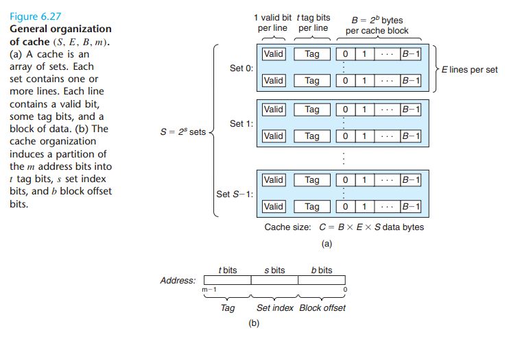
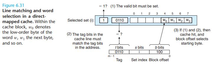
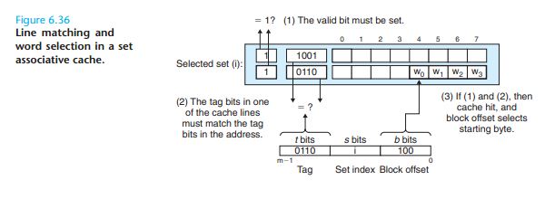
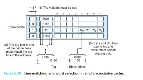
So how does the cache know whether it contains a copy of the word at address A?
Here is how it works:
The parameters S and B induce a partitioning of the m address bits into the three fields shown in Figure 6.27(b). The s set index bits in A form an index into the array of S sets. The first set is set 0, the second
set is set 1, and so on. When interpreted as an unsigned integer, the set index bits tell us which set the word must be stored in. Once we know which set the word must be contained in, the t tag bits in A tell us which line (if any) in the set contains the
word. A line in the set contains the word if and only if the valid bit is set and the tag bits in the line match the tag bits in the addressA. Once we have located the line identified by the tag in the set identified by the set index, then the b block offset
bits give us the offset of the word in the B -byte data block.
cache的设计简直把hash发挥到淋漓尽致的地步啊。。。
6.4.2 Direct-Mapped Caches
Caches are grouped into different classes based onE , the number of cache lines per set. A cache with exactly one line per set ( E = 1) is known as a direct-mapped cache (see Figure 6.29).Set Selection in Direct-Mapped Caches
In this step, the cache extracts the s set index bits from the middle of the address for w . These bits are interpreted as an unsigned integer that corresponds to a set number.
Why index with the middle bits?
You may be wondering why caches use the middle bits for the set index instead of the high-order bits. There is a good reason why the middle bits are better. Figure 6.33 shows why. If
the high-order bits are used as an index, then some contiguous memory blocks will map to the same cache set. For example, in
the figure, the first four blocks map to the first cache set, the second four blocks map to the second set,
and so on. If a program has good spatial locality and scans the elements of an array sequentially, then
the cache can only hold a block-sized chunk of the array at any point in time. This is an inefficient use of
the cache. Contrast this with middle-bit indexing, where adjacent blocks always map to different cache
lines. In this case, the cache can hold an entire C -sized chunk of the array, where C is the cache size
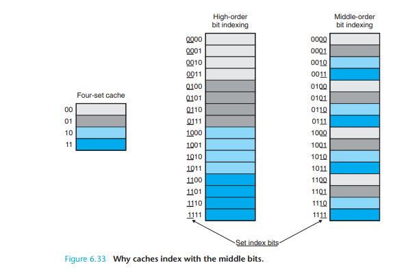
6.4.3 Set Associative Caches
A set associative cache relaxes this constraint so each set holds more than one cache line. A cache with 1 <E<C/B is often called an E -way set associative cache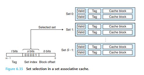
Line Matching and Word Selection in Set Associative Caches
6.4.4 Fully Associative Caches
6.4.5 Issues with Writes
what does it do about updating the copy of w in the next lower level of the hierarchy? The simplest approach, known aswrite-through , is to immediately write w ’s cache block tothe next lower level. While simple, write-through has the disadvantage of causing bus traffic with every write. Another approach, known aswrite-back, defers the update as long as possible by writing the updated block to the
next lower level only when it is evicted from the cache by the replacement algorithm.
Because of locality, write-back can significantly reduce the amount of bus traffic, but it has the disadvantage of additional complexity. The cache must maintain an additional dirty bit for each cache line that indicates
whether or not the cache block has been modified. Another issue is how to deal with write misses. One approach, known as write-allocate, loads the corresponding block from the next lower level into the cache and then updates the cache block.
As a rule, caches at lower levels of the memory hierarchy are more likely to use write-back instead of write-through because of the larger transfer times.
6.4.6 Anatomy of a Real Cache Hierarchy
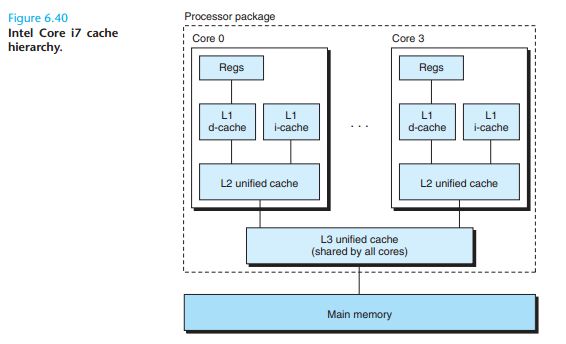
A cache that holds instructions only is called an i-cache . A cache that holds program data only is called a d-cache. A cache that holds both instructions and data is known as aunified cache . Modern processors include
separate i-caches and
d-caches. I-caches are typically read-only, and thus simpler. Also, having separate caches ensures that data accesses do not create conflict misses with instruction accesses, and vice versa, at the cost of a potential increase in capacity misses.
6.4.7 Performance Impact of Cache Parameters
Cache performance is evaluated with a number of metrics:Miss rate.The fraction of memory references during the execution of a pro-gram, or a part of a program, that miss. It is computed as # misses/# references.
Hit rate. The fraction of memory references that hit. It is computed as1−miss
rate.
Hit time. The time to deliver a word in the cache to the CPU, including the
time for set selection, line identification, and word selection. Hit time is on
the order of several clock cycles for L1 caches.
Miss penalty.Any additional time required because of a miss. The penalty for
L1 misses served from L2 is on the order of 10 cycles; from L3, 40 cycles; and
from main memory, 100 cycles
终于可以结了。。。。
于长沙橘子洲大桥


相关文章推荐
- 《CS:APP》 chapter 7 Linking 笔记
- 深入理解计算机系统_3e 第三章家庭作业 CS:APP3e chapter 3 homework
- 深入理解计算机系统_3e 第二章家庭作业 CS:APP3e chapter 2 homework
- 《CS:APP》 chapter 8 Exceptional Control Flow 笔记
- 深入理解计算机系统_3e 第六章家庭作业 CS:APP3e chapter 6 homework
- 深入理解计算机系统_3e 第四章家庭作业(部分) CS:APP3e chapter 4 homework
- 深入理解计算机系统_3e 第十一章家庭作业 CS:APP3e chapter 11 homework
- 深入理解计算机系统_3e 第八章家庭作业 CS:APP3e chapter 8 homework
- 深入理解计算机系统_3e 第五章家庭作业 CS:APP3e chapter 5 homework
- 《CS:APP》 chapter 8 Exceptional Control Flow 注意事项
- 《CS:APP》 chapter 3 Machine-Level Representation of Programs 笔记
- 深入理解计算机系统_3e 第十章家庭作业 CS:APP3e chapter 10 homework
- 《CS:APP》 chapter 2 Representing and Manipulating Information 笔记
- 《CS:APP》 chapter 1 A Tour of Computer Systems 笔记
- 深入理解计算机系统_3e 第七章家庭作业 CS:APP3e chapter 7 homework
- cs:app学习笔记(1):show-bytes
- App_Code/DataBase.cs(数据库操作类)